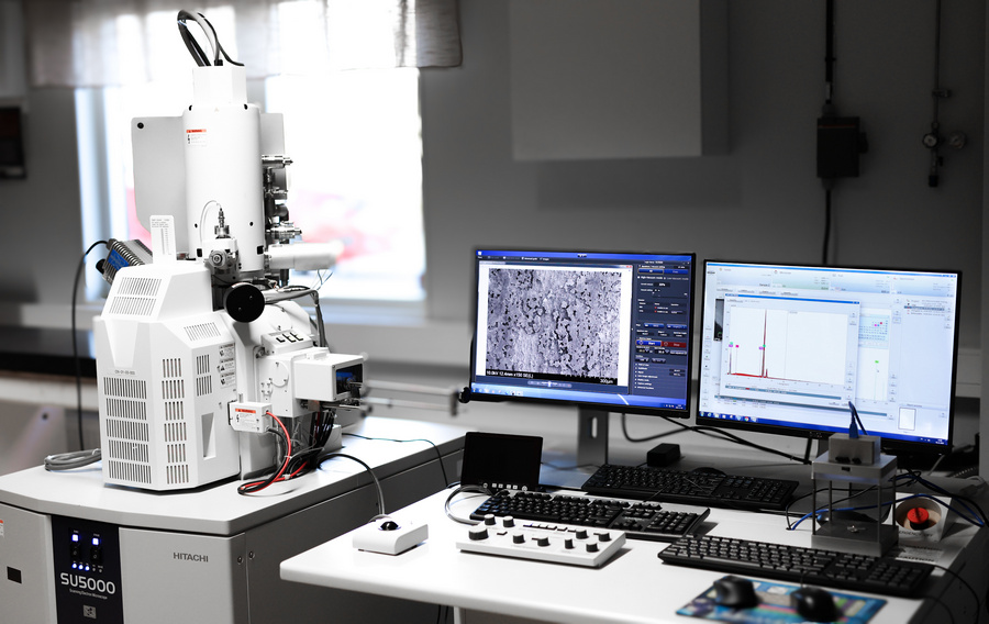
Scanning Electron Microscopy
Scanning electron microscopy (SEM) is a powerful technique for imaging features down to the nanometer range. SEM can provide topographical and compositional information and has a greater depth of field compared to conventional light optical microscopes.
Typical applications:
- Imaging of small features
- Spatial variations in chemical composition
- Enables chemical analysis (EDX)
- Fractography, an important part in failure investigations
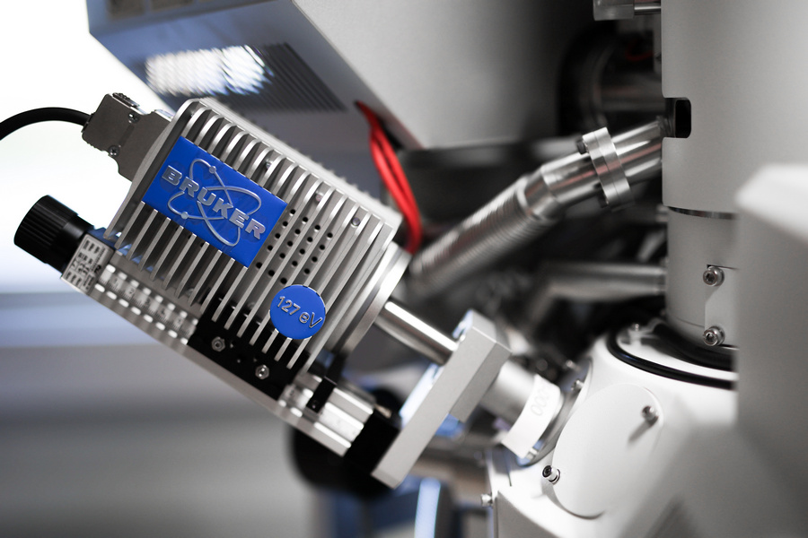
Energy Dispersive X-ray Spectroscopy (EDX)
Energy dispersive X-ray analysis (EDX) is a microanalysis technique that can be used for chemical characterization of the sample being analysed in SEM. EDX offers elemental identification and quantitative compositional information of features down to ~1 µm in size. EDX can be performed as point or area analysis, line scans and mappings.
Typical applications:
- Chemical analysis of thicker deposits, coatings and oxides
- Corrosion evaluation
- Identification of metallic materials